


Foreword: A photovoltaic inverter is a core unit of a new energy system. Its performance directly affects the power generation efficiency, the service life of the equipment and the quality of the grid-connected power grid. Voltage and current sensors, as important "sensing organs" in the inverter, monitor and feed back key parameters in real time, and transmit them to the CPU for collection and calculation. The program finally makes precise control according to the algorithm and preset conditions. The correct use of these devices plays an important role in ensuring the normal operation of the equipment. This paper systematically describes the application scenarios of voltage and current sensors in photovoltaic inverters and the selection strategies of some devices. Taking CHIPSENSE current/voltage sensor as an example.
Differences between string and centralized inverters:
The photovoltaic inverter system is divided into two types: string and centralized, and the difference between the two is not large. Centralized is a single high-power inverter, suitable for large ground power stations, with high bus voltage, generally 1500V, and even some have reached 2000V. The usual power is about 320KW, which is cost-effective.
String power is small, low voltage, flexible configuration and use. The bus is roughly 600V voltage and about 50KW power. These low-power inverters, the output voltage is finally connected together and integrated into the transmission grid for transmission.
It can also be understood that a 320KW centralized photovoltaic inverter is 10 string-type 32KW photovoltaic inverters connected in parallel; string-type and centralized inverters have their own advantages and disadvantages and exist simultaneously.
First. An overview of the inverter system and the core role of sensors
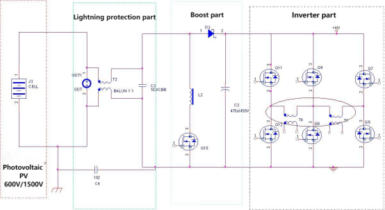
The photovoltaic inverter converts the direct current emitted by the photovoltaic array into alternating current through the high-speed switching action of power electronics, and finally provides various electrical equipment to the end point. Its typical topology includes DC input, lightning protection, DC/DC boost, DC/AC inverter, waveform shaping AC output and other major links. The correct use of voltage and current sensors in each link can play an important role, mainly depending on the goal pursued by the designer. CHIPSENSE current and voltage sensor as the same it. The overall block diagram is roughly as follows:
The core functions of voltage and current sensors in these aspects are:
Real-time monitoring:
The current and voltage parameters of the node are collected in real time and transmitted to the CPU, which makes high-speed A/D and converts analog signals into digital signals, providing a solid data foundation for the control algorithm and logic judgment of the program;
Closed-loop control, process:
The program detects voltage and current data, performs numerical operation and logic analysis and judgment, and then realizes precise closed-loop current sensor control of power devices (SiC /MOSFET/IGBT);
Fault protection and device protection:
The CPU detects and analyzes the output signals of the voltage and current sensor devices, and makes corresponding judgments of abnormal states such as overcurrent, short circuit, and leakage of the device, and then triggers the protection mechanism. This also requires the sensor to quickly respond to the primary signal;
Second. Practical Application of Voltage and Current Sensors in Each Link of inverter
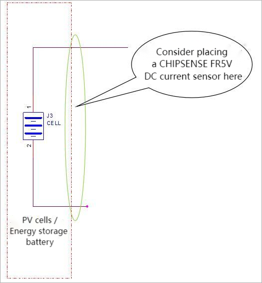
1. DC input link:
The DC power emitted by a single photovoltaic cell PV rises to 600V/1500V through channeling and parallel connection. Considering safety regulations, it is usually necessary to consider the leakage current monitoring of photovoltaic cell PV.
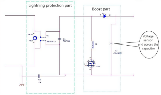
2. DC/DC boost and lightning protection:
DC/DC boost circuit is usually achieved by a complete circuit, generally do not need to deliberately pay attention to the voltage, but in order to meet the MPPT (Maximum Power Tracking); in the DC/DC input stage generally consider adding a voltage sensor. The string type because of its voltage is about 600V, so choose CHIPSENSE VN1V-1M-P01 voltage sensor, the device can detect the maximum voltage of 1100V;
Centralized because its voltage is as high as 1500V, CHIPSENSE VN1V-1M-P01 voltage sensor is not suitable, you can choose CHIPSENSE VN3A 2000 M15 voltage sensor.
The input stage usually needs lightning protection and surge protection to prevent damage to the back-end components and cause equipment abnormalities. The following circuits can meet the test of at least 4000V surge/EFT resistance. See the circuit below:
3. DC/AC inverter link:
This link requires attention to the control and fault protection of the IGBT bridge arm. Although the di2/dt value of IGBT is relatively high, it can withstand short-term overshoot currents better than MOS transistors. Generally, short-term overshoot is not easy to break, but it is expensive, especially for high-power devices.
In order to protect the power tube from being damaged, or to protect the upper and lower bridge arms from burning or even electrical fires due to damage to the power tube, it is necessary to place a high-precision, fast response time closed-loop Hall current sensor on the + HV bus, such as CHIPSENSE CN2A series current sensor, with a response time of less than 0.5 us and an accuracy of about 0.2%.
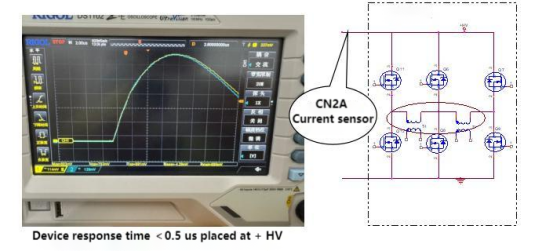
CHIPSENSE CN2A current sensor response time placed at + HV < 0.5us
This high-precision closed-loop Hall sensor from CHIPSENSE is placed here and serves two main functions: 1) to detect the total output current, which can be used to calculate and display the total output power; 2) to play a protective role similar to a fuse; once the MOS/IGBT of a bridge arm is damaged, it will inevitably lead to a direct connection between + HV and the ground, resulting in a short circuit. Such faults will be quickly detected.
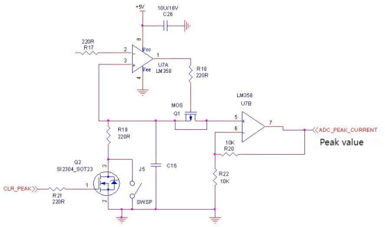
Although the response time of the closed-loop current sensor is < 0.5us, considering that the waveform data output by the inverter is generated by the program, which leads to a large program volume ratio, the CPU may not be able to quickly match the 0.5us response time. Raising the CPU's main frequency is a good way, but it is best to add a maximum value detection circuit. The analog value is converted into a high and low (H/L) level digital signal by means of a window comparator. The low level is normal, and the high level is faulty.
Finally, it is sent to the interrupt port of the CPU to achieve the fast response of the program and quickly cut off the output of the IGBT for the purpose of protection;
Considering that the response speed of the hardware circuit will be much higher than the operation and judgment of the program, then this protection signal can also be introduced into the enable terminal of the driver IC of the MOS/IGBT, which can be turned off faster than the program.
4.AC output link: synchronous grid connection and power quality.
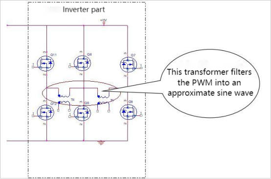
The load of the inverter, if it is a motor load, is generally directly connected to the output terminal; but if it is connected to the grid and supplies other electrical equipment, power supply, etc., an current sensor needs to be added to filter the PWM into a sine wave to improve the quality of power transmission. If necessary, a voltage sensor can also be placed here and placed in the front stage of the transformer.
Three. Application challenges and coping strategies in specific environments
Extreme cold environment (below -40 ° C)
Try to choose high-precision, low-temperature drift closed-loop Hall devices. The temperature drift of the device is less than 50ppm/℃, which can effectively avoid some false protection caused by temperature drift. A more reliable approach is to introduce the silicone rubber heating film/PTC heater commonly used in BMS systems. The program is used as the main control to control the start and stop of the heating film, and the mechanical thermostat is used as the secondary protection, which can effectively improve the operating reliability of the entire inverter device under the whole temperature environment.
Packaging: Devices are usually designed to meet IP67 requirements to better meet insulation voltage requirements
High current application scenario
The copper thickness of the PCB is usually 1oz, 2oz, 5oz, etc. Obviously, in order to flow through a large current, a larger copper cross-sectional area is required, so either widen the wiring or thicken the copper layer thickness. Or widen the line width and thicken the copper layer at the same time. Even if this is done, it will not only greatly increase the cost, but also it is difficult to meet the reliability requirements by relying on the PCB's wiring to run up to 100A of current: the heat generated by the copper layer cannot be dissipated under the wrapping of the PCB solder mask.
In this case, the Hall current sensor can be used to consider the wiring method. Up to 10mm2 of copper wire/copper bar can easily flow through 100A, and only the corresponding through-hole pads need to be opened on the PCB. This is a low-cost solution. CHIPSENSE current/voltage sensor is always centered on the customer's cost.
Higher isolation withstand voltage: The creepage distance design of the original secondary side of the device has considered the requirements of supporting systems above 1500V and can be used directly; CHIPSENSE can offer many kinds of current sensors.
Conclusion
Voltage and current sensors in photovoltaic inverters have gradually evolved from basic measurement components to core guarantee components that provide system safety and efficiency. As the PV voltage of photovoltaic cells rises from 600V to 1500V, and then up to 2000V, the switching frequency continues to increase, which is bound to promote the continuous evolution of sensors to higher accuracy, shorter response time and intelligence. In turn, it also further promotes the development of photovoltaic inverter systems towards more reliable and shorter maintenance time. CHIPSENSE will offer current/voltage sensor that can meet customer’s needs changes with the development of time.
CHIPSENSE is a national high-tech enterprise that focuses on the research and development, production, and application of high-end current and voltage sensors, as well as forward research on sensor chips and cutting-edge sensor technologies. CHIPSENSE is committed to providing customers with independently developed sensors, as well as diversified customized products and solutions.
“CHIPSENSE, sensing a better world!
www.chipsense.net